


SiP Design Capabilities
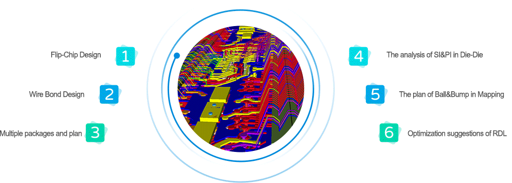
SiP Design Advantages
-Chip-Package-System Collaborative Planning and Design
-Simulation and design are conducted simultaneously
-Wire Bond 3D modeling
-High simulation accuracy and optimization
-Familiar with mainstream packaging substrate production process
-HSPICE model to IBIS model
-Assist in generating design instructions
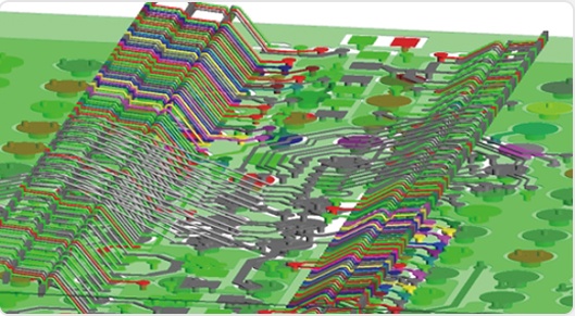
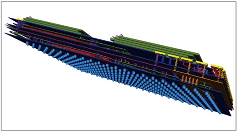
Sample SiP Design Case
- 9 DDR4 particles, 4+5 layers stacked
- DDR4 running speed 3200Mbps
- Overall performance comparable to SO-DIMM
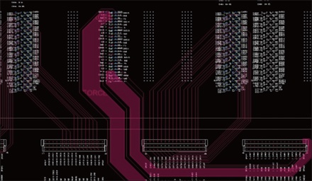
Automated Testing Board (ATE) Capabilities Introduction
- There are many pins of chips to be tested, up to thousands of pins
- More than 40 layers are stacked, and the plate thickness is more than 5mm
- The design and processing of wiring and through-hole tend to limit capacity
- Accurate simulation is required to ensure that the wiring will not affect the chip test accuracy